| Home | About Us | Contribute | Bookstore | Advertising | Subscribe for Free NOW! |
| News Archive | Features | Events | Recruitment | Directory |
News
19 October 2010
Eulitha unveils PHABLE UV litho technology for photonics patterning
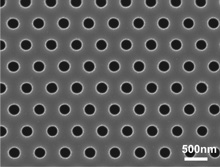 Nanolithography firm Eulitha AG, a spin-off of the Paul Scherrer Institute in Villigen, Switzerland, has unveiled its proprietary PHABLE (Photonics Enabler) mask-based ultraviolet (UV) photolithography technology for the low-cost, high-throughput fabrication of photonic nanostructures.
The firm says that this solves an ongoing problem in the fabrication of high-resolution photonic structures, since standard lithography equipment either lacks the required resolution or its cost is prohibitively high. The patented technology enables the formation of periodic nanostructures over large areas for applications such as LEDs, solar cells and flat-screen displays.
Eulitha says that, unlike currently available technologies, the PHABLE system forms an image that has practically unlimited depth of focus. Non-flat substrates, such as LED wafers, can hence be patterned uniformly and reproducibly. It also allows combinations of different patterns such as linear diffraction gratings and arrays of holes on hexagonal or square grids to be printed using a single exposure onto a chip or a wafer. The resolution of the printed features can be as small as one quarter of the illumination wavelength. The required masks can be produced inexpensively using standard chromium-on-quartz mask-writing technology. The technology will be presented at the 23rd International Microprocesses and Nanotechnology Conference (MNC 2010) in Fukuoka, Japan (9–12 November).
One of the major applications of the new technology involves photonic crystals, which are required to enhance the light extraction efficiency of LEDs. Unlike the nanoimprint method commonly employed for this purpose, it avoids contact between the mask and the wafer and does not require consumable soft-stamps, avoiding an expensive two-step process. Other applications are expected to also benefit from the development, including nanowire-based LEDs and photovoltaic devices, heteroepitaxy on patterned silicon substrates, and epitaxial lateral overgrowth (ELO) used in blue-ray lasers. Wire-grid polarizers, as required for both LCD displays and projectors, can also be produced.
PHABLE’s compatibility with conventional masks and UV exposure processing can smooth adoption by the industry, reckons Eulitha. Standard photoresists with suitable resolution and etch properties are available from multiple vendors, so manufacturers of HB-LEDs and other devices can rely on the usual, well-established sources for obtaining the required consumable materials, ensuring a low-cost manufacturing process for photonic nanostructures.
Eulitha is now offering samples and wafer batch processing services to companies and researchers developing nanostructure-based products who are interested in taking advantage of the technology. It is also offering laboratory lithography tools for 2–4” wafers that are suitable for product development. High-volume production tools with throughput in excess of 100 wafer-per-hour will be made available to manufacturers in the near future.
![]() Search: Photonics patterning LEDs ELO
Search: Photonics patterning LEDs ELO
UV photolithography
Visit: www.eulitha.com
For more: Latest issue of Semiconductor Today
![]() ©2010 Juno Publishing and Media Solutions Ltd. All rights reserved. Semiconductor Today and the editorial material contained within it and related media is the copyright of Juno Publishing and Media Solutions Ltd. Reproduction in whole or part without permission from Juno Publishing and Media Solutions Ltd is forbidden. In most cases, permission will be granted, if the author, magazine and publisher are acknowledged.
©2010 Juno Publishing and Media Solutions Ltd. All rights reserved. Semiconductor Today and the editorial material contained within it and related media is the copyright of Juno Publishing and Media Solutions Ltd. Reproduction in whole or part without permission from Juno Publishing and Media Solutions Ltd is forbidden. In most cases, permission will be granted, if the author, magazine and publisher are acknowledged.
Disclaimer: Material published within Semiconductor Today and related media does not necessarily reflect the views of the publisher or staff. Juno Publishing and Media Solutions Ltd and its staff accept no responsibility for opinions expressed, editorial errors and damage/injury to property or persons as a result of material published.
Semiconductor Today, Juno Publishing and Media Solutions Ltd, Suite no. 133, 20 Winchcombe Street, Cheltenham, GL52 2LY, UK
Web site by No Name No Slogan ![]()