| Home | About Us | Contribute | Bookstore | Advertising | Subscribe for Free NOW! |
| News Archive | Features | Events | Recruitment | Directory |
News
4 October 2010
Nitride LED output increased by up to 36% with distributed Bragg reflectors
Researchers in Korea have developed a distributed Bragg reflector (DBR) coating to boost light output from violet light-emitting diodes (LEDs) [K. H. Baik et al, J. Appl. Phys., vol108, p063105, 2010]. The researchers came from a number of institutions: Korea Electronics Technology Institute, Samsung Advanced Institute of Technology, Samsung LED, and Chonbuk National University. The research was supported by the New Growth Engine Smart Project Program funded by the Ministry of Knowledge Economy (MKE), Republic of Korea.
The researchers are seeking to contribute to improving solid-state lighting technology with the aim of making it a much more energy-efficient, longer-lasting, and more cost-effective than conventional lighting technologies so that LEDs will be implemented in general illumination applications, as well as in displays.
Much nitride LED research has focused on increasing the light extraction from LEDs, rather than improving the light generation efficiency. Recently, the flip-chip configuration has become popular, where light is emitted through the substrate on which the LED structures are grown. However, the generation of light in the active layers is not directed in a specific direction. To increase light output, it is necessary to reflect light going away from the substrate back into a useful direction.
DBRs use constructive interference of light waves to create reflection effects. The interference effects often come through creating precise layers of alternating materials with different refractive indices. DBRs are widely used to confine light in waveguides and optical fibers.
Another problem that arises with flip-chip light extraction is that reflection at the substrate-external interface can stop light leaving the device. The researchers used a patterned substrate for some of their devices. Patterned sapphire substrates can increase light extraction efficiency by reducing reflection back into the device at the substrate-external interface.
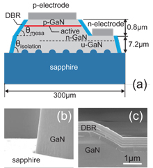 The LEDs (Figure 1) were grown on sapphire (unpatterned or with hemispherical patterning) using metal-organic chemical vapor deposition (MOCVD), starting with a 4.5μm undoped GaN layer, followed by 3μm of n-GaN. The active region consisted of a 5-period InGaN multi-quantum well (MQW) with GaN barriers. The electron-blocking layer was a combination of p-GaN and p-AlGaN. The nitride layers were completed with 0.14μm of p-GaN.
Figure 1: (a) Schematic cross-section of completed LEDs. (b) SEM images of isolation-etched mesa sidewall. (c) SEM cross-sections of shallow mesa sidewall, coated with five SiO2/TiO2 layer pairs forming DBR.
The layer construction was followed by inductively coupled-plasma reactive-ion etching (ICP-RIE) to create 300μm x 300μm isolation mesas (73° wall angle). The n-GaN layer was exposed by creating a shallow mesa on top of the isolation (26° wall angle) for deposition of the titanium/aluminum electrode. The p-electrode consisted of a reflective 300nm silver-copper layer. The 5x SiO2/TiO2 (73nm/38nm) DBR layer was deposited over the wafer using electron-beam evaporation. The contacts were exposed using ICP-RIE.
For packaging, the chips were flipped and bonded to silicon submounts and encapsulated in UV-epoxy using conventional 5mm packaging techniques. At 20mA drive current the peak emission wavelength was 400nm (violet).
The DBR structure was designed using optical transfer matrix calculations that suggested that 68nm/40nm SiO2/TiO2 quarter-wavelength layers would give the best results.
Various LED configurations were tested: no DBR, DBR on isolation walls only, and DBR on both isolation and shallow mesa sidewalls. These reflections directed the light emission through the sapphire substrate. These options were provided in LEDs grown on planar and patterned sapphire.
The output power of the planar LED without DBR (a) was taken as the normalization of 1 for the measurement set-up. The effect of adding DBR layers to the isolation wall (b) was to boost output by a factor of 1.29. Adding a DBR onto the shallow mesa wall (c) increased this to a 1.36 enhancement. The outputs for patterned sapphire LEDs were enhanced by factors of 1.75, 2.04 and 2.31 over the normalization device for planar sapphire diodes (a) with no DBR (A), DBR on isolation walls (B), and full DBR (C), respectively.
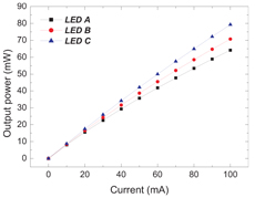 Figure 2: Optical output powers vs injection current of LEDs A, B, and C evaluated after conventional 5mm UV-epoxy packaging.
Packaged devices were created from the patterned LEDs and the output powers measured (Figure 2). At 20mA injection, the light output powers were 15.59mW, 16.54mW, and 17.52mW for LEDs A, B, and C, respectively. The reduction in the effectiveness of the DBR enhancement (1.12 = 17.52/15.59) is attributed to the effect of the epoxy refractive index (1.5) being intermediate to that of sapphire (1.8) and air (1).
![]() Search: DBR Violet LEDs Sapphire substrates MOCVD GaN InGaN MQW AlGaN
Search: DBR Violet LEDs Sapphire substrates MOCVD GaN InGaN MQW AlGaN
Visit: http://link.aip.org
For more: Latest issue of Semiconductor Today
The author Mike Cooke is a freelance technology journalist who has worked in the semiconductor and advanced technology sectors since 1997.
![]() ©2010 Juno Publishing and Media Solutions Ltd. All rights reserved. Semiconductor Today and the editorial material contained within it and related media is the copyright of Juno Publishing and Media Solutions Ltd. Reproduction in whole or part without permission from Juno Publishing and Media Solutions Ltd is forbidden. In most cases, permission will be granted, if the author, magazine and publisher are acknowledged.
©2010 Juno Publishing and Media Solutions Ltd. All rights reserved. Semiconductor Today and the editorial material contained within it and related media is the copyright of Juno Publishing and Media Solutions Ltd. Reproduction in whole or part without permission from Juno Publishing and Media Solutions Ltd is forbidden. In most cases, permission will be granted, if the author, magazine and publisher are acknowledged.
Disclaimer: Material published within Semiconductor Today and related media does not necessarily reflect the views of the publisher or staff. Juno Publishing and Media Solutions Ltd and its staff accept no responsibility for opinions expressed, editorial errors and damage/injury to property or persons as a result of material published.
Semiconductor Today, Juno Publishing and Media Solutions Ltd, Suite no. 133, 20 Winchcombe Street, Cheltenham, GL52 2LY, UK
Web site by No Name No Slogan ![]()