| Home | About Us | Contribute | Bookstore | Advertising | Subscribe for Free NOW! |
| News Archive | Features | Events | Recruitment | Directory |
News
5 November 2010
Varying wells to combat LED efficiency droop
Researchers at National Chiao-Tung University (NCTU) and Epistar Corp have used quantum wells with varying thickness to reduce ‘efficiency droop’ effects in indium gallium nitride (InGaN) blue light-emitting diodes (LEDs) [C. H. Wang et al, Appl. Phys. Lett., vol97, p181101, 2010].
Nitride semiconductors are the dominant material for making devices emitting light with shorter wavelengths (<540nm) of green, blue, violet and ultra-violet. These devices work at high efficiency at relatively low current but, as the current increases, the efficiency tends to fall off for various reasons, particularly with the longer-wavelength region (green). Overcoming this problem would enable lower-cost LED lighting installations to work with less power consumption.
Multi-quantum well structures with InGaN wells and GaN (or sometimes InGaN with a different composition) are used to create light emission, with one side injecting holes and the other electrons. It has been found that, while the electrons travel across the structure fairly evenly (or overshooting into the p-contact/hole source region), the holes tend to be concentrated near the p-injection contact.
By making the wells wider towards the p-contact, the NCTU/Epistar group hoped to improve the hole concentration across the active region. The hole carrier lifetime in thicker wells tends to be longer, allowing a larger proportion to move on to the next well.
The researchers grew their nitride LED structures using metal-organic chemical vapor deposition (MOCVD) on c-plane sapphire. The base for the MQW structures was a 4nm GaN nucleation layer followed by a 4μm n-GaN buffer.
On top of this, a superlattice was constructed using 10x InGaN/GaN pairs. The graded-thickness MQW (GQW) structure consisted of InGaN (In molar fraction 15%) quantum wells with 10nm GaN barriers. The well thicknesses were 1.5, 1.8, 2.1, 2.4, 2.7 and 3nm, as determined by the growth time. A reference LED with constant thickness wells was also produced with a well thickness of 2.25nm, a value that makes the active volume equal for the graded and ungraded structures.
The p-contact layers consisted of an electron-blocking layer of 20nm AlGaN (15% Al) and 200nm of p-GaN. These epitaxial structures with transparent indium tin oxide (ITO) contact layers applied were formed into 300μm x 300μm LED mesas. Nickel-gold was applied for the contact pads.
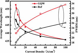 Figure 1: Average wavelength and FWHM as a function of current density for reference and GQW LEDs.
The electroluminescent (EL) testing of the devices showed the GQW device to be red-shifted relative to the reference up to 100A/cm2 current density (Figure 1). Also, the width of the emission line is wider. However, over this energy range the blue-shift with increasing current is greater in the GQW device, so that the emission wavelengths of the two devices are approximately equal at 100A/cm2.
Normally, LED blue-shift is attributed to band-filling effects making the energy difference between electron and hole levels greater (and hence increasing the recombination photon energy). Also, charge screening effects can play a role. These effects arise from the quantum-confined Stark effect (QCSE), where piezoelectric polarization fields are developed from the strained nature of the wells. Increases in the full-width at half maximum (FWHM) of emissions are often attributed to band filling and self-heating.
For the GQW devices, based on simulations, the researchers believe that the increased blue-shift is due to more recombination occurring in the narrower wells as the current density increases. Since the wells emit at somewhat different wavelengths, the symmetry of the spectral peak gives information about the balance of recombination across the structure.
The asymmetry factor (AsF = FWHM divided by twice the distance from the low wavelength intersect to the peak, giving 1 for a symmetric peak) for the regular LED changed from 1.04 to 0.98 as the current increased from a density of 1A/cm2 to 100A/cm2. The GQW devices change from 1.05 to 0.89 over the same range. The low AsF value shows increased contribution from the blue-end and decreased contribution from the red-end of the spectral distribution.
The researchers comment: ‘These enormous changes in wavelength and linewidth might make the design of the GQW concept impractical for lighting applications.’
Future work for the group could include grading the indium content of the wells to compensate somewhat for these undesired effects. This could be done by reducing the indium content of the wider wells.
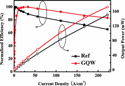 Figure 2: Comparison of normalized EL efficiency and light output power (L) curves vs current density.
The researchers also measured the effect on efficiency droop (Figure 2). The light output power of the GQW was 24.3mW, compared with 18.0mW for the reference device, at 20A/cm2. It was also found that grading increases the point at which the efficiency droop starts (30A/cm2 vs 2A/cm2 in the reference) and reduces the fall off after that point (16% drop from peak at 200A/cm2 vs 32%).
The researchers suggest that the improved hole distribution and consequent reduction of Auger effects that kick in at high carrier concentrations lead to better recombination rates into photons rather than other mechanisms.
See related items:
Trapezoid wells effect reduced LED droop and lower cross-over pointSemipolar blue LED with 39.5% external quantum efficiency
InAlN provides better electron-blocking layer in nitride LEDs
Tunneling a way to understand efficiency droop in InGaN LEDs
Auger largely responsible for limited LED efficiency
InGaN LED spillover and efficiency droop
![]() Search: NCTU Epistar Quantum wells Efficiency droop InGaN Blue LEDs
Search: NCTU Epistar Quantum wells Efficiency droop InGaN Blue LEDs
Visit: http://link.aip.org
Visit: http://www.epistar.com.tw/about-e.htm
For more: Latest issue of Semiconductor Today
The author Mike Cooke is a freelance technology journalist who has worked in the semiconductor and advanced technology sectors since 1997.
![]() ©2010 Juno Publishing and Media Solutions Ltd. All rights reserved. Semiconductor Today and the editorial material contained within it and related media is the copyright of Juno Publishing and Media Solutions Ltd. Reproduction in whole or part without permission from Juno Publishing and Media Solutions Ltd is forbidden. In most cases, permission will be granted, if the author, magazine and publisher are acknowledged.
©2010 Juno Publishing and Media Solutions Ltd. All rights reserved. Semiconductor Today and the editorial material contained within it and related media is the copyright of Juno Publishing and Media Solutions Ltd. Reproduction in whole or part without permission from Juno Publishing and Media Solutions Ltd is forbidden. In most cases, permission will be granted, if the author, magazine and publisher are acknowledged.
Disclaimer: Material published within Semiconductor Today and related media does not necessarily reflect the views of the publisher or staff. Juno Publishing and Media Solutions Ltd and its staff accept no responsibility for opinions expressed, editorial errors and damage/injury to property or persons as a result of material published.
Semiconductor Today, Juno Publishing and Media Solutions Ltd, Suite no. 133, 20 Winchcombe Street, Cheltenham, GL52 2LY, UK
Web site by No Name No Slogan ![]()