| Home | About Us | Contribute | Bookstore | Advertising | Subscribe for Free NOW! |
| News Archive | Features | Events | Recruitment | Directory |
News
4 June 2010
Fujitsu develops record low-noise transistor for millimeter-band receivers
Japan’s Fujitsu Ltd and Fujitsu Laboratories Ltd has announced the development of an indium phosphide-based high-electron-mobility transistor (InP HEMT) using their proprietary ‘space cavity’ structure that, operating at the millimeter-band frequency of 94GHz, reduces the noise level generated by the transistor by about 30% to 0.7dB (compared with previous InP HEMT technology presented by Fujitsu at the IEEE MTT-S International Microwave Symposium 2007). This results in what is claimed to be record low noise levels. Details are being presented at this week’s 22nd International Conference on Indium Phosphide and Related Materials (IPRM 2010) in Takamatsu, Kagawa Prefecture, Japan (31 May – 4 June).
Fujitsu’s noise-lowering technology should enable sensitivity enhancements in millimeter-band receivers (which allow image sensors — operating primarily in the 35 or 94GHz bands for anti-terrorist initiatives at major airports — to capture data in the form of heat radiated by objects). This in turn should enable the time required for image capture to be almost halved.
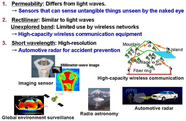
Figure 1: Features and applications of millimeter waves.
In contrast to infrared or optical signals, radio waves in the millimeter band (30–300GHz) are permeable and able to travel through thin walls and fabric. As part of anti-terrorism prevention efforts, major airports are considering deploying image sensors that take advantage of the permeability of millimeter-waves.
The new technology can enable the extension of high-capacity wireless transmission reach by 20% (to on a par with optical transmission). In addition, as the commercial use of wireless networks is limited and thus makes it easy to secure large swaths of bandwidth, millimeter-wave signals are suitable for transmitting very large volumes of data exceeding several gigabits per second.
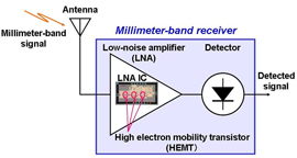 Figure 2: Structure of Fujitsu’s millimeter-band receiver.
High-capacity millimeter-band wireless transmission equipment can therefore be used in place of trunk lines in locations where it is difficult to install fiber-optic cabling (helping to narrow the economic differences between people or regions with good access to information and communications technology versus those with poor access).
Image sensors must be able to detect very weak millimeter-waves emitted by people or objects, and high-capacity millimeter-band transceiver equipment needs to be able to detect signals that have weakened in the process of being transmitted and dispersed through the air. So, for both of these applications there is a need for high-sensitivity millimeter-band transceivers that can receive very weak millimeter-wave signals.
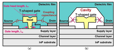
Figure 3: Conventional InP HEMT (a) and InP HEMT with ‘space cavity’ (b).
To make a millimeter-band transceiver highly sensitive, in the HEMT in the transceiver’s amplifier it is necessary to control the noise that is generated along with high signal amplification rates. If the noise level in the HEMT is high, the noise interferes with reception, making detection of weak signals impossible.
Until now, the conventional method for achieving high signal amplification rates with low noise was to miniaturize the HEMT. However, this requires specialized fabrication equipment, and progress was limited due to low yields and poor uniformity. The challenge was hence to find an alternative method for achieving high signal amplification rates with low noise.
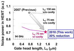 Figure 4: Effect of Fujitsu’s new developed technology for reducing transistor noise (94GHz).
Based on an analysis of the mechanisms by which noise is generated, Fujitsu developed novel technology with the following features to reduce noise:
- In conventional InP HEMTs, if the coupling capacitance between the gate and the source or drain is large, the millimeter-band signal amplification rates fall. Fujitsu hence eliminated the inter-layer dielectric film around the gate electrode, forming a ‘space cavity’ that reduces the coupling capacitance. The technology was developed under a research contract from Japan's Ministry of Internal Affairs and Communications with the aim of increasing the speed of InP HEMTs and, for the first time, Fujitsu verified that reducing the coupling capacitance through the introduction of this 'space cavity' structure also reduces noise.
- Since the gate electrode is the source of noise in a HEMT, reducing the gate resistance is an effective method for reducing noise. HEMTs for the lower frequencies used in transceivers for home satellite broadcast systems hence use a T-shaped gate, with a low-resistance head electrode placed on the upper part of a micro-electrode to reduce gate resistance and noise.
However, when using a low-resistance T-shaped gate in the 94GHz band, because the distance between the T-shaped gate and the source or drain is narrowed, there is an increase in noise from coupling capacitance. Using the ‘space cavity’ structure, Fujitsu has now confirmed that, even in the 94GHz band, coupling capacitance is reduced when using the T-shaped gate. Moreover, Fujitsu also verified that increasing the length of the T-shaped gate’s head also reduces noise.
Using the new technology, Fujitsu fabricated an InP HEMT with a gate length of 75nm that reduced the noise figure by 30% (compared to previous technologies) to the record low of 0.7dB.
Fujitsu plans to equip high-performance image sensors and high-capacity transmission equipment with amplifiers that use the new low-noise InP HEMT, targeting practical-use commercialization for 2012. Fujitsu also aims to expand the range of applications into areas such as radio astronomy and environmental monitoring of the earth.
Part of the research was conducted under the contract ‘Research and Development Project for Expansion of Radio Spectrum Resources’ sponsored by Japan’s Ministry of Internal Affairs and Communications.
Visit: http://jp.fujitsu.com/labs/en
![]() ©2010 Juno Publishing and Media Solutions Ltd. All rights reserved. Semiconductor Today and the editorial material contained within it and related media is the copyright of Juno Publishing and Media Solutions Ltd. Reproduction in whole or part without permission from Juno Publishing and Media Solutions Ltd is forbidden. In most cases, permission will be granted, if the author, magazine and publisher are acknowledged.
©2010 Juno Publishing and Media Solutions Ltd. All rights reserved. Semiconductor Today and the editorial material contained within it and related media is the copyright of Juno Publishing and Media Solutions Ltd. Reproduction in whole or part without permission from Juno Publishing and Media Solutions Ltd is forbidden. In most cases, permission will be granted, if the author, magazine and publisher are acknowledged.
Disclaimer: Material published within Semiconductor Today and related media does not necessarily reflect the views of the publisher or staff. Juno Publishing and Media Solutions Ltd and its staff accept no responsibility for opinions expressed, editorial errors and damage/injury to property or persons as a result of material published.
Semiconductor Today, Juno Publishing and Media Solutions Ltd, Suite no. 133, 20 Winchcombe Street, Cheltenham, GL52 2LY, UK
Web site by No Name No Slogan ![]()