| Home | About Us | Contribute | Bookstore | Advertising | Subscribe for Free NOW! |
| News Archive | Features | Events | Recruitment | Directory |
News
1 February 2010
Getting closer to improve QWFET performance
Researchers from Taiwan and Japan have developed a new process for creating narrower ohmic source–drain contacts for indium arsenide (InAs) quantum well field-effect transistors (QWFETs) [Chien-I Kuo et al, Jpn. J. Appl. Phys., vol49, p010212, 2010].
QWFETs on indium phosphide are attractive for sub-millimeter applications due to their excellent high-frequency performance, enabled by high electron mobility and high saturation velocity. Such devices are also being explored for incorporation into the silicon mainstream, where low power consumption and high-speed digital logic properties are sought with possible application in the middle of the coming decade (about 2015, ‘beyond the 22nm node’).
At present, while the gate lengths of such QWFETs are of the orders of tens of nanometers, the source and drain contact separations (S/D separations) are much larger (1500-3000nm/1.5-3.0μm). One reason for this separation is the need to reduce parasitic resistances through making large contacts.
The researchers from National Chiao-Tung University, Yuan Ze University and Tokyo Institute of Technology have developed a modified self-aligned gate (SAG) process tailored to the needs of III-V materials rather than silicon. The development of the SAG process for silicon metal-oxide-semiconductor field-effect transistors (MOSFETs) in the 1960s was one of the key steps in creating the dominance of that technology in electronics and for enabling the almost incredible shrinkage of components that has taken place in the ensuing decades.
Unfortunately, the traditional SAG process requires ion implantation of doping materials, followed by annealing at high temperatures, sometimes as high as 1000°C. The aim of annealing is to repair the crystal structure and ‘activate’ the dopants, creating high-mobility charge carriers. Such processes are not suitable for most III-V devices. Implantations damage the heterostructure layers that have been carefully built up to make the quantum wells and so on. Further, the annealing temperatures are close to those used in the III-V material growth processes. Grain regrowth and the creation of hot carriers at high temperatures make subsequent device failure more likely.
The modified SAG process uses simple re-deposition of ohmic metal. ‘The measurement results in this work clearly evidenced that superior device performance can be easily achieved through a few added simple fabrication processes,’ the researchers claim.
The process was used to make 70nm gate-length InAs QWFETs with an effective source–drain separation of only 650nm. The researchers believe that the technique is suitable for mass production, needing just a few added simple steps.
The InAs QWFET structure was grown using molecular-beam epitaxy (MBE) on 2-inch diameter indium phosphide (InP) wafers (500nm InAlAs buffer, 3nm In0.53Ga0.47As low sub-channel, 5nm InAs channel, 2nm In0.53Ga0.47As upper sub-channel, 3nm InAlAs spacer with silicon delta-doping, 5nm InAlAs Schottky barrier, 4nm InP etch stop, 40nm n-type In0.53Ga0.47As cap).
The device mesa was formed using wet chemical etching. Ohmic contacts with 3000nm spacing were made by successively evaporating gold, germanium, nickel and gold (Au/Ge/Ni/Au) onto the heavily doped cap layer. The 70nm T-shape gate was then formed.
Silicon dioxide was then applied using plasma-enhanced chemical vapor deposition (PECVD) as a 150nm hard mask to create a region for electron-gun evaporation re-deposition of ohmic gold metal onto the n-type cap layer between the source and drain, reducing the effective separation (Figure 1). A 60nm-thick silicon nitride passivation was then deposited using PECVD.
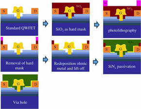 Figure 1: QWFET process flow for reducing the effective source–drain separation.
With zero gate voltage (VGS) a saturation current density
(IDS) of 517mA/mm was obtained for the 650nm S/D separation devices at a source–drain voltage (VDS) of 0.5V. The drain current under the same conditions was 391mA/mm with a 3000nm S/D separation device. The extracted source resistances were 5Ω and 1.1Ω for the 3000nm and 650nm S/D separation devices, respectively.
 A slight impact of the reduced distance between the source and drain is a marginal reduction of the breakdown voltage (VDG,BR) from 3.6V to 3.4V due to the increased electric field between the gate and drain. However, this breakdown is acceptable for low-voltage applications. Fringing capacitance was also increased from 36.76fF to 44.47fF — an effect that could be reduced by optimizing the device layout, the researchers hope.
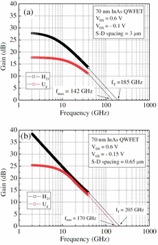
Figure 2: Frequency dependence of current gain H21 and Mason’s unilateral gain (Ug) of InAs channel QWFETs with 3000nm (a) and 650nm (b) S/D spacings. Frequency range: 2-40GHz,
VDS = 0.6V.
The current-gain cut-off (fT) was 205GHz for the 650nm device, compared with 185GHz for the 3000nm transistor. The maximum oscillation frequencies (fmax) were 170GHz and 142GHz, respectively. The improved high-frequency performance was attributed to the reduction in source resistance and an increase in transconductance (gm) from 946mS/mm to 1348mS/mm at a VDS of 0.5V.
See related item:
Mid-decade timescale for compound/silicon semiconductor integration
![]() Search: InP QWFETs InP MBE
Search: InP QWFETs InP MBE
Visit: http://jjap.ipap.jp/link?JJAP/49/010212
The author Mike Cooke is a freelance technology journalist who has worked in the semiconductor and advanced technology sectors since 1997.
![]() ©2010 Juno Publishing and Media Solutions Ltd. All rights reserved. Semiconductor Today and the editorial material contained within it and related media is the copyright of Juno Publishing and Media Solutions Ltd. Reproduction in whole or part without permission from Juno Publishing and Media Solutions Ltd is forbidden. In most cases, permission will be granted, if the author, magazine and publisher are acknowledged.
©2010 Juno Publishing and Media Solutions Ltd. All rights reserved. Semiconductor Today and the editorial material contained within it and related media is the copyright of Juno Publishing and Media Solutions Ltd. Reproduction in whole or part without permission from Juno Publishing and Media Solutions Ltd is forbidden. In most cases, permission will be granted, if the author, magazine and publisher are acknowledged.
Disclaimer: Material published within Semiconductor Today and related media does not necessarily reflect the views of the publisher or staff. Juno Publishing and Media Solutions Ltd and its staff accept no responsibility for opinions expressed, editorial errors and damage/injury to property or persons as a result of material published.
Semiconductor Today, Juno Publishing and Media Solutions Ltd, Suite no. 133, 20 Winchcombe Street, Cheltenham, GL52 2LY, UK
Web site by No Name No Slogan ![]()