| Home | About Us | Contribute | Bookstore | Advertising | Subscribe for Free NOW! |
| News Archive | Features | Events | Recruitment | Directory |
News
2 February 2010
Stopping nitride HEMT buffer leaks
Polarization in nitride semiconductor devices is often seen as a problem, particularly where light emission is required (e.g. in lasers, light-emitting diodes). By contrast, University of Notre Dame researchers [Yu Cao et al, Appl. Phys. Lett., vol96, p042102, 2010] see opportunities to create highly insulating layers for use in high-electron-mobility transistors (HEMTs). Nitride semiconductor HEMTs are being widely developed for high-speed and high-power applications.
The Notre Dame work focused on blocking leakage through the buffer layer of the HEMT that arises through shallow dopant impurities such as silicon (Si) or oxygen (O) at the interface with the substrate, which can be made of silicon carbide (SiC) or semi-insulating gallium nitride (SI GaN). The presence of this conducting region under the buffer impacts both on/off ratios for digital applications and device speed where high performance is needed.
Notre Dame produced two HEMTs – one designed to show the problem of buffer leakage and the other a solution that uses giant polarization fields in nitride semiconductors to create a highly insulating layer (Figure 1). The devices were grown using radio-frequency (RF) plasma-source molecular beam epitaxy (MBE) on commercial Ga-face GaN templates (2μm iron-doped SI GaN layer on sapphire substrate).
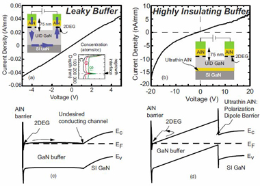
Figure 1: Leakage current density in buffer vs applied voltage for control sample (a, inset: SIMS atomic concentrations against depth with strong impurity peaks of Si, O and C at re-growth interface). Using ultra-thin AlN nucleation layer (b) gives much lower buffer leakage. Energy band diagrams of the two structures from AlN top barrier (left end of diagrams) down to SI GaN template (right end). Adding AlN nucleation layer at right end (d) removes unwanted conduction path in (c).
For the leaky device (Figure 1, left), two monolayers of gallium were deposited on the Ga-face to create a metal-rich nucleation layer under the ~234nm of unintentionally doped GaN, followed by a 3nm aluminum nitride (AlN) cap. A two-dimensional electron gas (2DEG) forms through polarization effects at the GaN/AlN interface.
For the measurement of buffer leakage, the region of the 2DEG between the electrodes is cut with a reactive ion etch (RIE) so that current must flow through the unintentional paths such as the buffer/template interface. The leaky device has a current flow of 40mA/mm at ±5V. This flow is a factor of 25 smaller than that typical in an on-state GaN HEMT and hence would significantly limit on/off ratios. Secondary-ion mass spectrometry (SIMS) reveals large peaks for carbon, silicon and oxygen – the latter two elements are known to be n-type dopants in GaN.
An insulating device is created by growing an ultrathin AlN nucleation layer (NL) before the GaN buffer (Figure 1, right). This cuts the leakage to less than 20nA/mm at 20V. At 4V, the leakage is reduced by seven orders of magnitude (a factor of 107), compared with the leaky set-up.
It was found in further experiments that nitrogen-rich growth conditions of the AlN were critical to insulating properties. A metal-rich AlN layer leads to leakage, possibly due to the diffusion of oxygen and silicon dopant atoms from the re-growth interface into the buffer layer.
Actual HEMTs were built with and without the AlN nucleation layer (Figure 2). The on/off ratio improves from about 100 for the leaky device to 106 for the device with AlN nucleation layer. The researchers point out that this is a desirable feature for both analog (RF) and digital (power-switching) applications, adding: “In addition, the natural back-barrier introduced due to the band offsets and polarization dipole, as shown in the energy band diagram in Figure 1(d), can potentially enable reduced short-channel effects for shorter-gate-length HEMTs”. The sub-threshold slope is also steeper with the AlN NL: 300mV/dec rather than 650mV/dec.
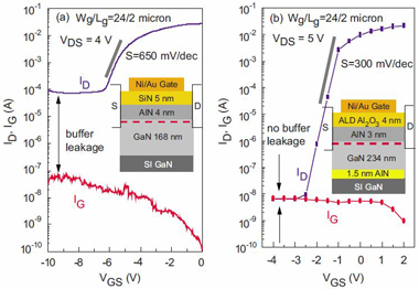
Figure 2: Transfer characteristics of leaky control sample (a) with severe buffer leakage, and of sample with AlN nucleation layer (b) cutting buffer leakage so that it is lower than the gate leakage.
Among the advantages that Notre Dame sees for its approach are the absence of a dopant, and savings on source materials and in growth time.
![]() Search: GaN HEMTs GaN SiC MBE AlN
Search: GaN HEMTs GaN SiC MBE AlN
Visit: http://link.aip.org/link/?APPLAB/96/042102/1
The author Mike Cooke is a freelance technology journalist who has worked in the semiconductor and advanced technology sectors since 1997.

![]() ©2010 Juno Publishing and Media Solutions Ltd. All rights reserved. Semiconductor Today and the editorial material contained within it and related media is the copyright of Juno Publishing and Media Solutions Ltd. Reproduction in whole or part without permission from Juno Publishing and Media Solutions Ltd is forbidden. In most cases, permission will be granted, if the author, magazine and publisher are acknowledged.
©2010 Juno Publishing and Media Solutions Ltd. All rights reserved. Semiconductor Today and the editorial material contained within it and related media is the copyright of Juno Publishing and Media Solutions Ltd. Reproduction in whole or part without permission from Juno Publishing and Media Solutions Ltd is forbidden. In most cases, permission will be granted, if the author, magazine and publisher are acknowledged.
Disclaimer: Material published within Semiconductor Today and related media does not necessarily reflect the views of the publisher or staff. Juno Publishing and Media Solutions Ltd and its staff accept no responsibility for opinions expressed, editorial errors and damage/injury to property or persons as a result of material published.
Semiconductor Today, Juno Publishing and Media Solutions Ltd, Suite no. 133, 20 Winchcombe Street, Cheltenham, GL52 2LY, UK
Web site by No Name No Slogan ![]()