| Home | About Us | Contribute | Bookstore | Advertising | Subscribe for Free NOW! |
| News Archive | Features | Events | Recruitment | Directory |
News
6 August 2010
UCSB reports first packaged blue LEDs on (30-3-1) nitride substrates
University of California Santa Barbara (UCSB) researchers have reported data on what are claimed to be the first blue (452nm) packaged high-power/efficiency semi-polar (30-3-1) nitride light-emitting diodes (LEDs) [Ingrid L. Koslow et al, Jpn. J. Appl. Phys., vol49, p080203, 2010]. In the past year, UCSB has been developing LEDs and laser diodes using a number of different semipolar crystal orientations in efforts to improve performance over traditional polar c-plane devices.
With maximum external quantum efficiencies (EQEs) that can be of the order of 60%, c-plane devices can seem hard to beat. Some of this is the advantage of maturity – growing material in other crystal directions is still at a relatively early stage, meaning that these materials tend to have higher defect levels (~1010/cm2) compared with c-plane. The operating conditions can also be rather special to create headline EQEs (e.g. a particular current, temperature control, etc.). What are needed are devices that can operate at high efficiency and power over a broad range of operating conditions.
It is believed that non-polar and semi-polar materials may produce better devices because the electric fields across the active region are reduced. In polar devices, these fields cause a ‘quantum-confined Stark effect’ (QCSE), separating the electrons and holes and hence making the lifetime for radiative recombination longer compared with other mechanisms, hence reducing efficiency. The fields can arise from spontaneous and piezoelectric (i.e. strain-dependent) polarization in nitride semiconductors.
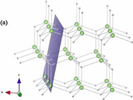 The UCSB researchers note that the (30-3-1) plane used in their latest work is only 5° away in crystal orientation from (20-21) material that has recently shown promise for green laser diodes at Sumitomo Electric Industries in Japan (Figure 1).
Figure 1: Schematic of (30-3-1) crystal plane.
UCSB works with Japan’s Mitsubishi Chemical, which supplied the free-standing (30-3-1) semi-polar substrates, grown by hydride vapor phase epitaxy (HVPE). Based on its measurements, the manufacturer estimates a threading dislocation density of less than 5x10⁶/cm2 for the material. The substrate was polished using chemical and mechanical processes.
UCSB performed its metal-organic chemical vapor deposition (MOCVD) under atmospheric pressure, using conditions similar to those employed for growing c-plane LEDs, with silicon providing n-type and magnesium p-type doping. The structure (Figure 2) was fairly typical for indium gallium nitride (InGaN) LEDs with a three-period multi-quantum well InGaN/GaN (3nm/20nm) light-emitting active region (Figure 1).
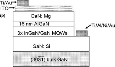
Figure 2: Schematic of (30-3-1) LED device structure.
A 16nm p-AlGaN (aluminum gallium nitride) layer was used to block electrons from overshooting the active region. Without an electron-blocking layer, GaN LEDs generally exhibit reduced efficiency, as electron–hole recombination in the p-contact region is non-radiative or at a parasitic wavelength.
The n-GaN layer was grown at 1140°C, the active region at 870°C and the p-GaN at 960–990°C.
Tin oxide-doped indium oxide (SnO2-doped In2O3, indium tin oxide/ITO) transparent conducting material was applied to the p-GaN to spread the current from the p-electrode. The LED contact structures were applied to 200μm x 500μm mesas using conventional means. The mesas were formed using a chlorine-based inductively coupled plasma etch.
The wafers were thinned and then scribed to release the individual devices. The LEDs were put on silver headers and encapsulated in silicone with a truncated cone format.
Measurements were carried out using DC current, and the power and emission spectra were determined using an integrating sphere. The peak EQE for the device was found to be 27.8% at 5mA injection current. At 20mA, the EQE was 26.5% and the output power was 14.48mW. The forward voltage at 20mA was 5.4V, which is seen as being a little higher than desired. The researchers see this as being due to unoptimized growth conditions for the final p-GaN and ITO layers.
Spectral measurements indicate a peak wavelength red-shift of less than 1nm for currents in the range 5–100mA. This small shift is typical for devices grown on non-polar and semi-polar (10-1-1) substrates. By contrast, devices grown on traditional c-plane GaN have blue-shifts of tens of nanometers (an effect attributed to energy shifts in the band structure arising from the quantum confined Stark effect).
The full-width at half-maximum (FWHM) of the emission spectrum is less than 25nm at low current. This increases at higher currents to ~33nm at 100mA. The researchers see this behavior and the small red-shift in peak wavelength as being due to thermal effects arising from the inefficiencies indicated by the high forward voltage.
The researchers conclude: “Although LED growth on this plane has not yet been optimized, these results demonstrate the viability of high-performance GaN LEDs and laser diodes grown on substrates of this orientation.”
![]() Search: Blue LEDs GaN substrates InGaN/GaN MQWs AlGaN
Search: Blue LEDs GaN substrates InGaN/GaN MQWs AlGaN
Visit: http://jjap.ipap.jp/link?JJAP/49/080203
The author Mike Cooke is a freelance technology journalist who has worked in the semiconductor and advanced technology sectors since 1997.
![]() ©2010 Juno Publishing and Media Solutions Ltd. All rights reserved. Semiconductor Today and the editorial material contained within it and related media is the copyright of Juno Publishing and Media Solutions Ltd. Reproduction in whole or part without permission from Juno Publishing and Media Solutions Ltd is forbidden. In most cases, permission will be granted, if the author, magazine and publisher are acknowledged.
©2010 Juno Publishing and Media Solutions Ltd. All rights reserved. Semiconductor Today and the editorial material contained within it and related media is the copyright of Juno Publishing and Media Solutions Ltd. Reproduction in whole or part without permission from Juno Publishing and Media Solutions Ltd is forbidden. In most cases, permission will be granted, if the author, magazine and publisher are acknowledged.
Disclaimer: Material published within Semiconductor Today and related media does not necessarily reflect the views of the publisher or staff. Juno Publishing and Media Solutions Ltd and its staff accept no responsibility for opinions expressed, editorial errors and damage/injury to property or persons as a result of material published.
Semiconductor Today, Juno Publishing and Media Solutions Ltd, Suite no. 133, 20 Winchcombe Street, Cheltenham, GL52 2LY, UK
Web site by No Name No Slogan ![]()