| Home | About Us | Contribute | Bookstore | Advertising | Subscribe for Free NOW! |
| News Archive | Features | Events | Recruitment | Directory |
News
28 April 2010
Sumitomo powers up vertical nitride transistor technology
Researchers at Japan’s Sumitomo Electric Industries (SEI) have developed a new nitride semiconductor vertical transistor structure with a view to power applications [Masaya Okada et al, Appl. Phys. Express, vol3, p054201, 2010]. Until recently vertical structures have been difficult to realize for nitride semiconductor systems, particularly those grown on insulating sapphire.
Nitride semiconductor transistors are attractive for power applications due to high breakdown fields and high electron saturation velocities. However, the planar format of high-electron-mobility transistors (HEMTs) is not ideal from a power handling perspective. Despite this, HEMTs have been developed for wireless base-station power amplifiers, power supplies, power conditioners for green energy, and inverters for automobiles.
Vertical structures should enable lower specific on-resistance, high breakdown voltages and high current flow, since the flow is not restricted to a thin layer, but rather travels down through the wafer structure.
SEI has taken advantage of newly available free-standing gallium nitride substrates with low dislocation densities to realize its vertical heterostructure field-effect transistor (VHFET) using a sloped two-dimensional electron gas (2DEG) as the channel (Figure 1). SEI produces 50mm-diameter GaN crystal substrates using its own vapor-phase technique.
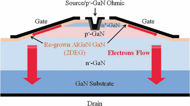
Figure 1: Sumitomo Electric Industries’ VHFET with re-grown AlGaN/GaN two-dimensional electron gas channels on GaN substrate.
The new VHFET device can be arranged to be normally-off, which is an attractive feature for reduced power consumption. The specific on-resistance achieved was as low as 7.6mΩ-cm2, while the (hard) breakdown voltage was 672V. Reasonable current blocking was maintained up to more than 600V.
The epitaxial layers of the device were grown using metal-organic chemical vapor deposition (MOCVD) on c-plane GaN substrates. Silicon (Si) and magnesium (Mg) were used for n- and p-doping, respectively. The layer thicknesses were 5μm for the n--GaN (Si 7x10¹⁵/cm3), 1μm for the p--GaN (Mg 5x10¹⁸/cm3) and 0.2μm for the n+-GaN (Si 3x10¹⁸/cm3).
To create the sloped channels (Figure 2), mesa structures with a slope angle of about 16° were formed using inductively coupled plasma-reactive ion etching (ICP-RIE). The 2DEG was then formed by MOCVD re-growth on the slopes of undoped GaN (75nm) and aluminum gallium nitride (Al0.2Ga0.8N, 10–35nm). Standard photolithography and lift-off was used to form the electrodes. The source and drain contacts consisted of Al-based ohmic material. A Schottky nickel–gold contact was used for the gate.
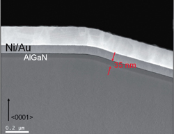 Figure 2: Transmission electron micrograph (TEM) of re-grown AlGaN layer on slope of mesa structure.
The researchers comment that their specific on-resistance is lower than that achieved previously by other groups (e.g. 9.3mΩ-cm2, Rohm, reported in 2008) attempting to create vertical MOSFETs using nitride semiconductors. SEI believes that this is due to the channel using a 2DEG, rather than an inversion layer.
The researchers believe that the specific on-resistance can be further lowered, to near the theoretical drift limit for nitride semiconductors, by improving material quality, shortening the channel length, down-scaling the structures, and increasing the packing density.
The threshold voltage was controlled by the thickness of the AlGaN layer. The normally-off threshold of +0.3V was achieved with 10nm of AlGaN. The researchers say that the 3V threshold required for power applications should be possible with an insulated, rather than Schottky gate scheme.
![]() Search: Sumitomo Electric Industries GaN substrates AlGaN/GaN MOCVD
Search: Sumitomo Electric Industries GaN substrates AlGaN/GaN MOCVD
Visit: http://apex.ipap.jp/link?APEX/3/054201
Visit: http://global-sei.com/index.html
The author Mike Cooke is a freelance technology journalist who has worked in the semiconductor and advanced technology sectors since 1997.
![]() ©2010 Juno Publishing and Media Solutions Ltd. All rights reserved. Semiconductor Today and the editorial material contained within it and related media is the copyright of Juno Publishing and Media Solutions Ltd. Reproduction in whole or part without permission from Juno Publishing and Media Solutions Ltd is forbidden. In most cases, permission will be granted, if the author, magazine and publisher are acknowledged.
©2010 Juno Publishing and Media Solutions Ltd. All rights reserved. Semiconductor Today and the editorial material contained within it and related media is the copyright of Juno Publishing and Media Solutions Ltd. Reproduction in whole or part without permission from Juno Publishing and Media Solutions Ltd is forbidden. In most cases, permission will be granted, if the author, magazine and publisher are acknowledged.
Disclaimer: Material published within Semiconductor Today and related media does not necessarily reflect the views of the publisher or staff. Juno Publishing and Media Solutions Ltd and its staff accept no responsibility for opinions expressed, editorial errors and damage/injury to property or persons as a result of material published.
Semiconductor Today, Juno Publishing and Media Solutions Ltd, Suite no. 133, 20 Winchcombe Street, Cheltenham, GL52 2LY, UK
Web site by No Name No Slogan ![]()