| Home | About Us | Contribute | Bookstore | Advertising | Subscribe for Free NOW! |
| News Archive | Features | Events | Recruitment | Directory |
| FREE subscription |
| Subscribe for free to receive each issue of Semiconductor Today magazine and weekly news brief. |
News
10 March 2009
HVPE of semi-polar GaN on m-plane sapphire boosts opto device performance
The technical team at Oxford Instruments-TDI, led by Dr Alexander Usikov, says that it has made significant progress in fabricating semi-polar gallium nitride layers for optoelectronic devices (which should increase radiative recombination efficiency and device performance), and is working closely with a leading LED manufacturer.
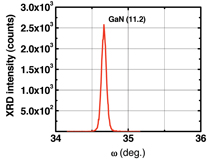
Graph: demonstrates the XRD w-scan rocking curve of symmetric (11.2) reflex measured for a 2-inch (11.2) GaN/m-plane sapphire wafer.
In the past decade, group III-nitride materials have been widely used for visible and ultraviolet LEDs and blue-violet laser diodes. Most of these optoelectronic devices are typically fabricated on conventional polar (0001) c-plane oriented substrate materials. However, devices grown on a polar substrate orientation suffer undesirable spontaneous and piezoelectric polarization, resulting in significant bending of the energy bands in the quantum well layers of the structure. This reduces radiative recombination efficiency, limiting the light-emission performance.
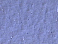
Picture: the optical micrograph (image width of 60μm) of (11.2) oriented GaN layer grown on m-plane sapphire. Atomic force microscope (AFM) results show the rms surface roughness of 3.7nm for a 2μm x2μm scan.
To diminish these polarization effects, the growth of GaN-related devices along semi-polar and non-polar directions has been studied intensively. Using hydride vapour phase epitaxy (HVPE), the Oxford Instruments-TDI team has grown high-quality, semi-polar (11.2) oriented GaN on (10.0) m-plane sapphire with an intermediate layer between the sapphire substrate and the GaN layer.
The semi-polar (11.2) GaN layers were grown in the temperature range 930-1050ºC in an inert argon ambient at atmospheric pressure. Gallium and aluminum were used as metallic source materials and hydrogen chloride (HCl) and ammonia (NH3) as the active gases for the HVPE process. The epitaxial growth of GaN was performed at a rate of about 60μm/ hour using an intermediate layer deposited on m-plane sapphire followed by an undoped GaN layer.
The firm says that this growth procedure results in a high-quality, semi-polar GaN layer with a thickness of up to 30μm.
See related items:
OIPT wins order from Asian HB-LED maker for first three of up to 15 systems
Oxford Instruments maintains full-year expectations
Riber buys OIPT’s MBE business
Oxford Instruments acquires TDI
See: Oxford Instruments Company Profile
![]() Search: Oxford Instruments TDI LEDs Blue-violet laser diodes HVPE GaN Sapphire
Search: Oxford Instruments TDI LEDs Blue-violet laser diodes HVPE GaN Sapphire
Visit: www.oxford-instruments.com

![]() ©2009 Juno Publishing and Media Solutions Ltd. All rights reserved. Semiconductor Today and the editorial material contained within it and related media is the copyright of Juno Publishing and Media Solutions Ltd. Reproduction in whole or part without permission from Juno Publishing and Media Solutions Ltd is forbidden. In most cases, permission will be granted, if the author, magazine and publisher are acknowledged.
©2009 Juno Publishing and Media Solutions Ltd. All rights reserved. Semiconductor Today and the editorial material contained within it and related media is the copyright of Juno Publishing and Media Solutions Ltd. Reproduction in whole or part without permission from Juno Publishing and Media Solutions Ltd is forbidden. In most cases, permission will be granted, if the author, magazine and publisher are acknowledged.
Disclaimer: Material published within Semiconductor Today and related media does not necessarily reflect the views of the publisher or staff. Juno Publishing and Media Solutions Ltd and its staff accept no responsibility for opinions expressed, editorial errors and damage/injury to property or persons as a result of material published.
Semiconductor Today, Juno Publishing and Media Solutions Ltd, Suite no. 133, 20 Winchcombe Street, Cheltenham, GL52 2LY, UK
Web site by No Name No Slogan ![]()