| Home | About Us | Contribute | Bookstore | Advertising | Subscribe for Free NOW! |
| News Archive | Features | Events | Recruitment | Directory |
| FREE subscription |
| Subscribe for free to receive each issue of Semiconductor Today magazine and weekly news brief. |
News
14 July 2009
Optimizing InP substrate orientation for 1.55µm InAs QD telecom lasers
Researchers based in France at the Institut National des Sciences Appliquées (INSA) de Rennes have been investigating the optimal substrate orientation for creating indium arsenide (InAs) quantum dots on indium phosphide (InP), with 1.55µm communication laser wavelengths being the aim [Elias et al, Japanese Journal of Applied Physics, vol.48, p.070204, 2009].
Quantum dot (QD) lasers are expected to enable high-speed modulation, low threshold current and high characteristic temperature (allowing higher-temperature operation). Some success in this respect has been achieved in producing InAs dots on gallium arsenide (GaAs) substrates that lase at wavelengths of 0.9-1.4µm.
For 1.55µm, the InAs/InP system is seen as being more suitable in terms of the resulting dot sizes due to the lower lattice mismatch between the materials (3.2%) compared with GaAs-based dots (7.2%). Unfortunately, rather than forming round dots of suitable size (~25nm diameter), growth tends to result in either a high density of wires/dashes (extended in the [1-10] lattice direction) or dots that are too large (50nm diameter).
Previous work at INSA has used InP substrates oriented in the high-index (113)B plane direction rather than more usual low-index (001), achieving smaller dots (~25nm diameter) and low threshold current. However, such substrates are difficult to incorporate into standard InP production technology.
The new approach is to use substrates that are cut off the (001) InP crystal ingot with a somewhat misoriented surface, which reduces the tendency to form wires, dashes or larger dots. The investigation involved comparing the structures produced with misorientations of about 2 degrees in the (111)A or (111)B surfaces, along with a nominal (001) control.
A Riber 32 gas-source molecular-beam epitaxy (GS-MBE) system was used to create the QD structures. It was found that the arsenic flux is also critical for producing QDs. The buffer layer on which the dots were grown was Ga0.2In0.8As0.435P0.565, which is lattice matched to the InP substrate. The emission wavelength of the buffer layer is 1.18µm.
A high flow of 6 standard cubic centimeters (sccm) of the arsine (AsH3) source gas (resulting in an As flux of about 30 times the In flux) leads in all cases to large dots (60-65nm base diameter). However, 0.3sccm of AsH3 results in smaller isotropic dots on the B-surface substrates. The 2nm-high dots measure 30-35nm in diameter and are produced with a density of 7x10¹⁰ QDs/cm2. The dot height varies by about 30%, irrespective of the arsine flow rate.
The 1nm-high structures grown on nominal and A-surface substrates are elongated in the [1-10] direction. The elongations are 200-500nm and 100-200nm for the nominal and A-surface substrates, respectively.
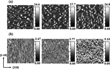
Picture: Atomic force microscopy of InAs structures produced with arsine flow rates of (a) 6sccm and (b) 0.3sccm. The scan field is 1µm x 1µm.
Focusing on B-surface substrates, a variation of temperature was then investigated, growing dots at 400ºC and 450ºC in addition to the 480ºC of the previous experiments with the range of substrates and flow rates. The lower arsine flow rate was naturally used. A modest increase in dot density to 9x10¹⁰ QDs/cm2, and a decrease in dimensions to 26nm diameter and 1nm height was achieved.
A double capping process, using the same Ga0.2In0.8As0.435P0.565 material composition as in the buffer layer, allows tuning of the photoluminescence of the 480ºC QDs to emission wavelengths close to the 1.55µm target. In addition, inhomogeneous broadening is much reduced – a desirable feature for laser development.
A 1mm cavity laser structure consisting of five QD layers separated by Ga0.2In0.8As0.435P0.565 spacers was grown that produced room-temperature electroluminescence at 1.62µm. The lasing threshold current density was 1.06kA/cm2 (206A/cm2 per layer). The device measured 1mm x 0.1mm. The output power is not reported.
The researchers see these results as being comparable to those of Alcatel-Thales researchers, who achieved a 110A/cm2 per layer current density threshold for an InAs quantum dash laser on nominal InP(001) substrates.
![]() Search: InP substrates InAs quantum dots
Search: InP substrates InAs quantum dots
Visit: http://foton.insa-rennes.fr/efoton-insa.html
Visit: http://jjap.ipap.jp/link?JJAP/48/070204
The author Mike Cooke is a freelance technology journalist who has worked in the semiconductor and advanced technology sectors since 1997.
![]() ©2009 Juno Publishing and Media Solutions Ltd. All rights reserved. Semiconductor Today and the editorial material contained within it and related media is the copyright of Juno Publishing and Media Solutions Ltd. Reproduction in whole or part without permission from Juno Publishing and Media Solutions Ltd is forbidden. In most cases, permission will be granted, if the author, magazine and publisher are acknowledged.
©2009 Juno Publishing and Media Solutions Ltd. All rights reserved. Semiconductor Today and the editorial material contained within it and related media is the copyright of Juno Publishing and Media Solutions Ltd. Reproduction in whole or part without permission from Juno Publishing and Media Solutions Ltd is forbidden. In most cases, permission will be granted, if the author, magazine and publisher are acknowledged.
Disclaimer: Material published within Semiconductor Today and related media does not necessarily reflect the views of the publisher or staff. Juno Publishing and Media Solutions Ltd and its staff accept no responsibility for opinions expressed, editorial errors and damage/injury to property or persons as a result of material published.
Semiconductor Today, Juno Publishing and Media Solutions Ltd, Suite no. 133, 20 Winchcombe Street, Cheltenham, GL52 2LY, UK
Web site by No Name No Slogan ![]()