| Home | About Us | Contribute | Bookstore | Advertising | Subscribe for Free NOW! |
| News Archive | Features | Events | Recruitment | Directory |
| FREE subscription |
| Subscribe for free to receive each issue of Semiconductor Today magazine and weekly news brief. |
News
15 July 2009
IMEC launches industrial affiliation program on GaN-on-Si technology
International research center IMEC of Leuven, Belgium has launched a new industrial affiliation program (IIAP) focusing on the development of gallium nitride technology for both power conversion and solid-state lighting applications. A key goal is to lower the cost of GaN technology by using large-diameter (up to 200mm) silicon wafers and hence by leveraging silicon's scale of economics.
Due to their unique combination of excellent transport properties and high electrical field operation capability, GaN-based devices can overcome the intrinsic material limits of silicon MOSFET structures which, for some applications, are being reached in traditional high-voltage power devices.
The few GaN devices on the market are based on AlGaN/GaN high-electron mobility transistor (HEMT) structures and are normally-on devices, designed for RF applications, e.g. in wireless communication. The IIAP envisages the next generation of power electronics components, requiring the development of normally-off devices (for safety reasons) with high-voltage breakdown (600-1000V) and low on-resistance, operating in enhancement mode.
 The scope of the IIAP is therefore to develop high-voltage, low-loss, high-power switching devices based on large-diameter GaN-on-Si technology. Potential applications include high-power switching in solar converters, motor drives, hybrid electrical vehicles or switch-mode power supplies.
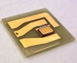
Figure 1: IMEC’s SiN/AlGaN/GaN double-heterostructure FET, demonstrating breakdown voltages up to 1000V.
A second sub-program of the IIAP will exploit GaN-on-Si technology for the development of high-efficiency, high-power white LEDs. Key issues are enhancing the external and internal quantum efficiencies and enabling high-current operation. III-nitrides in general exhibit excellent light-emission properties in a very broad range of the visible and ultraviolet (UV) spectrum. However, LED illumination using these devices can only become broadly acceptable if new high-volume manufacturing technologies are developed that yield LEDs with luminous efficacies of 150lm/W. IMEC says that its proprietary thin-film texture LED technology will be used on GaN-on-Si LEDs to enhance the external quantum efficiency.
A common challenge for both power electronics and optoelectronics is cost reduction. “GaN on large-diameter Si wafers (from 100mm and 150mm towards 200mm) in combination with CMOS-compatible processes offers the best perspective to create economically viable solutions,” says GaN program director Marianne Germain. While very few players can currently process GaN on large-diameter Si wafers, IMEC - in collaboration with Aixtron - has recently demonstrated crack-free GaN growth on 200mm wafers. “Also, for other challenges the IIAP can build on IMEC’s 10 years’ experience in GaN technology, including unique skills in epi-layer growth, new device concept, device integration and a thin-film textured LED technology for high-efficiency III-nitride LEDs,” adds Germain.
 IMEC says it invites both integrated device manufacturers and the compound semiconductor industry to join the program, enabling partners to build on IMEC’s expertise in GaN and benefit from a sharing of cost, risk, talent and intellectual property.
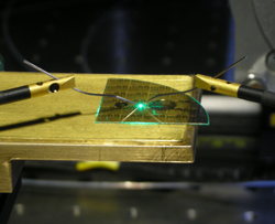
Figure 2: IMEC’s green LEDs on sapphire.
Visit: www.imec.be
![]() ©2009 Juno Publishing and Media Solutions Ltd. All rights reserved. Semiconductor Today and the editorial material contained within it and related media is the copyright of Juno Publishing and Media Solutions Ltd. Reproduction in whole or part without permission from Juno Publishing and Media Solutions Ltd is forbidden. In most cases, permission will be granted, if the author, magazine and publisher are acknowledged.
©2009 Juno Publishing and Media Solutions Ltd. All rights reserved. Semiconductor Today and the editorial material contained within it and related media is the copyright of Juno Publishing and Media Solutions Ltd. Reproduction in whole or part without permission from Juno Publishing and Media Solutions Ltd is forbidden. In most cases, permission will be granted, if the author, magazine and publisher are acknowledged.
Disclaimer: Material published within Semiconductor Today and related media does not necessarily reflect the views of the publisher or staff. Juno Publishing and Media Solutions Ltd and its staff accept no responsibility for opinions expressed, editorial errors and damage/injury to property or persons as a result of material published.
Semiconductor Today, Juno Publishing and Media Solutions Ltd, Suite no. 133, 20 Winchcombe Street, Cheltenham, GL52 2LY, UK
Web site by No Name No Slogan ![]()