


News: Optoelectronics
25 March 2024
Coherent announces first 6-inch InP scalable wafer fabs
Materials, networking and laser technology firm Coherent Corp of Saxonburg, PA, USA has established what it says is the world’s first capability for 6-inch indium phosphide (InP) wafer fabrication, in its fabs in Sherman, Texas, and Järfälla, Sweden.
The expansion enables the firm to increase production capacity and lower die costs for InP optoelectronic devices, which are widely used in applications such as coherent optical communications, datacom transceivers, artificial intelligence (AI) interconnects, advanced sensing for consumer electronics and wearables, medical and automotive applications and, in the future, in 6G wireless and satellite communications networks.
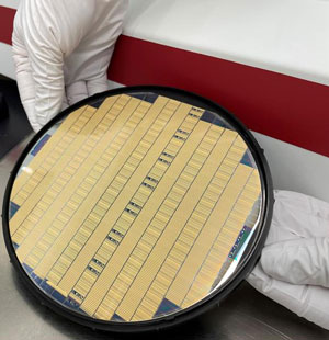 Picture: Coherent InP wafer.
The development is “a result of our continuous investment in innovation and technology development, and our years of investment and operating experience in high-volume vertical-cavity surface-emitting laser (VCSEL) array manufacturing for mobile handsets,” says Dr Giovanni Barbarossa, chief strategy officer and president, Materials Segment. “Vertical integration at scale is a core strategy that we have been relying upon in several of our markets, and it has enabled our optoelectronics products to win in the marketplace by delivering world-class quality, performance, time-to-market, and cost advantage,” he adds.
“Moving to 6-inch wafers will enable us to continue to deliver massive productivity improvements, including manufacturing 4x the number of devices per wafer, achieve a greater than 60% reduction in die cost, and allow us to transition our fabs to higher-capacity, more-efficient automated process tools,” says Dr Beck Mason, executive VP, Telecommunications. “This capability will allow us to meet the growing demand for our indium phosphide products in several of our core markets, while enhancing our competitiveness and profitability.”
Coherent is in the process of qualifying several existing products on its 6-inch InP platform, including a 200G electro-absorption modulated laser (EML), 200G distributed-feedback laser and Mach–Zehnder modulator (DFB-MZ), 100G EML, high-speed photodetectors, and high-power continuous-wave (CW) lasers for silicon photonics applications. The company expects to transition the bulk of its production from 3-inch InP to 6-inch InP in the next few years to fully leverage the benefits of larger wafer size, higher yield, and improved performance that will be required to provide a sustainable competitive advantage in its communications and sensing markets.