


News: Microelectronics
21 March 2024
Layer transfer of III-N MEMS through 2D hexagonal boron nitride
Researchers based in France and the USA report on the extension of two-dimensional (2D) material-based layer transfer to simple fabrication of free-standing III-nitride micro-electro-mechanical systems (MEMS) on silicon [Rajat Gujrati et al, Appl. Phys. Lett., v124, p104102, 2024]
The team from the GT-CNRS International Research Lab collaboration between Georgia Institute of Technology in the USA and France’s CNRS government research organization, along with the Université de Bordeaux and the LAAS-CNRS systems research laboratory, comments: “The realization of flexible III-N MEMS, which are difficult to manufacture through conventional micro-machining processes, would open the door to a wide range of applications, from wearable devices for health monitoring to the Internet of Things, even if further technical developments are needed to reach the level of yield and device performance offered by conventional fabrication methods.”
The researchers suggest that the methods could be extended to flexible substrates, such as polyethylene terephthalate (PET) or Kapton.
Apart from the wide bandgaps exhibited by III-nitride materials such as aluminium gallium nitride (AlGaN), they also feature important piezoelectric and piezoresistive characteristics, high temperature stability, chemical robustness, and potential for GaN electronics integration. AlGaN/GaN structures also generate a thin ‘two-dimensional electron gas’ (2DEG) near the interface of the two materials. The 2DEG is a key component of high-electron-mobility transistors (HEMTs), operating as channel between source and drain. The 2DEG formation is also attractive in a MEMS sensor context, where it can function as a strain transducer.
Reports of GaN MEMS structures include Lamb wave resonators, infrared detection, and electronic filters. Layer-transfer techniques enable high-quality growth on reusable substrates, lowering production costs.
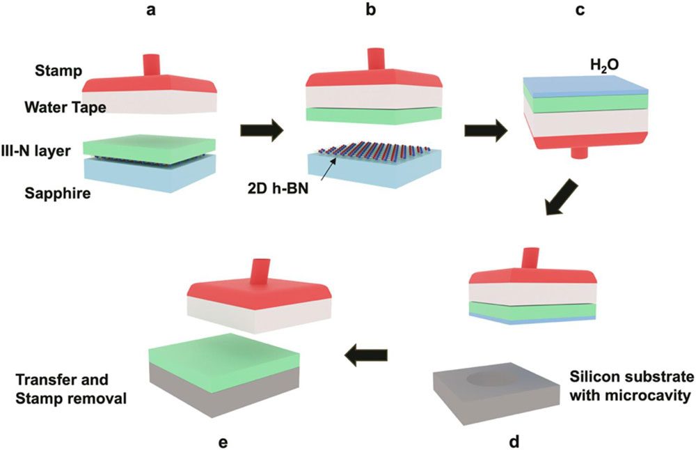
Figure 1: (a, b) Water-soluble adhesive tape used to pick up epilayer grown on h-BN/sapphire template. (c, d) Epilayer transferred using pressure and capillary forces onto silicon substrate with etched cavities and (e) tape dissolved to obtain III-N structure held to silicon substrate by van der Waals forces.
The researchers used a pick-and-place method to fabricate free-standing III-N MEMS structures on silicon (Figure 1). The III-nitride material was grown on a hexagonal boron nitride (hBN) layer on sapphire and transferred to a micro-cavity in a silicon substrate. The growth method was metal-organic chemical vapor deposition (MOCVD). Two samples were produced: one with 300nm GaN and 300nm AlGaN layers on 3nm hBN, and the other with 2.5μm hBN.
The hBN consists of 2D layers of atoms held together by covalent forces. The weaker van der Waals forces between the layers enables relatively easy separation of the material grown on the hBN.
A 15mmx15mm stamp with double-sided water-soluble adhesive tape on its surface picked the III-N from the growth substrate. The underside of the III-N structure was wetted with a water-soaked lens wipe before placing in 22μm-deep micro-cavities deep reactive-ion etched (DRIE) into a silicon substrate. The wetting enabled ‘capillary assembly’, where “the drying of a water film at the interface of the III-N film and the substrate is used to create a large surface area to promote adhesion via van der Waals forces,” the team explains.
The stamp was removed by dissolving the tape by immersion in a water-filled beaker for 30 minutes.
The researchers studied the material structures’ mechanical properties by placing the assemblies on lead zirconate titanate (PZT) piezoelectric actuators (Figure 2). Excitations were detected using laser Doppler vibrometry. The lowest mode frequencies for a GaN/AlGaN structure in a 180μmx60μm cavity were 1.39MHz, 1.58MHz and 1.85MHz, respectively. Finite-element method simulations with typical Young’s modulus values for the component materials (261GPa EGaN, 285GPa EAlGaN) gave corresponding values of 1.25MHz, 1.39MHz and 1.65MHz. The 2nd/3rd mode ratios relative to the 1st mode were 1.14/1.33 experimentally, and 1.11/1.32 in simulation.
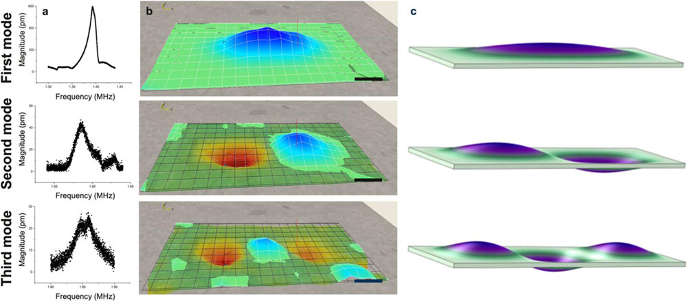
Figure 2: (a) Resonance spectra of first three modes of rectangular AlGaN/GaN plate on silicon at largest displacement location; (b) corresponding measured 3D displacement maps showing maximum deflection amplitude (scale bars: 20μm); and (c) COMSOL simulations.
The mechanical behavior of hBN in a 450μmx150μm format was more difficult to interpret. Single-layer hBN has a Young’s modulus of about 0.8TPa. Thicker layers, beyond 8 mono-layers, show a much reduced value. The modulus value extracted from the behavior of the hBN plate was 18GPa. The researchers also varied some other parameters in an attempt to fit the experimental data with a higher Young’s modulus of 120GPa, “the lowest value found in the literature”. In particular, the researchers studied the possibilities of residual stress in the plate, and a smaller effective size of the plate. Neither hypothesis gave a fully satisfactory explanation of the observations.
https://doi.org/10.1063/5.0191772
http://research.georgiatech-europe.eu/
The author Mike Cooke is a freelance technology journalist who has worked in the semiconductor and advanced technology sectors since 1997.