


News: Optoelectronics
23 February 2024
Triple-lattice photonic crystal laser
China’s Changchun Institute of Optics, Fine Mechanics and Physics, and University of Chinese Academy of Sciences have reported continuous-wave operation of a 1550nm low-threshold triple-lattice photonic-crystal surface-emitting laser (PCSEL) on indium phosphide (InP) substrate [Ziye Wang et al, Light: Science & Applications, v13, p44, 2024].
The team comments: “Our results present an opportunity for InP-based high-speed 1.557μm PCSELs, which are expected to play an essential role in high-speed optical communication and LiDAR applications.”
The 1.55μm range transmits though optical fiber with minimum loss, and features eye-safety up to higher power. However, traditional lasers suffer from poor performance due to high interband absorption in this range. The PCSEL structure can deliver strong optical feedback to overcome this, reducing thresholds and improving output power.
Photonic crystals consist of two-dimensional structures of different refractive index that create in-plane resonance from interference of the reflected light waves.
The researchers explain: “Light amplification and lasing are realized at the band edge by forming a broad-area standing wave in the lateral direction, with the light extracted from the normal direction by first-order diffraction. A narrow-divergence far-field pattern can be achieved due to the broad-area coherent resonance.”
The researchers used a photonic crystal of holes filled with low-refractive-index InP in a triple-lattice formation (three holes per unit cell). A higher index contrast could be achieved with air-voids, but such structures suffer from manufacturability and reliability problems.
The team comments: “We believe that PCSELs with smaller cavity and lower threshold current can be obtained by combining the advantages of strong feedback of triple-lattice photonic crystal and high dielectric contrast of void-containing resonator, if the manufacturability and reliability are solved in future.”
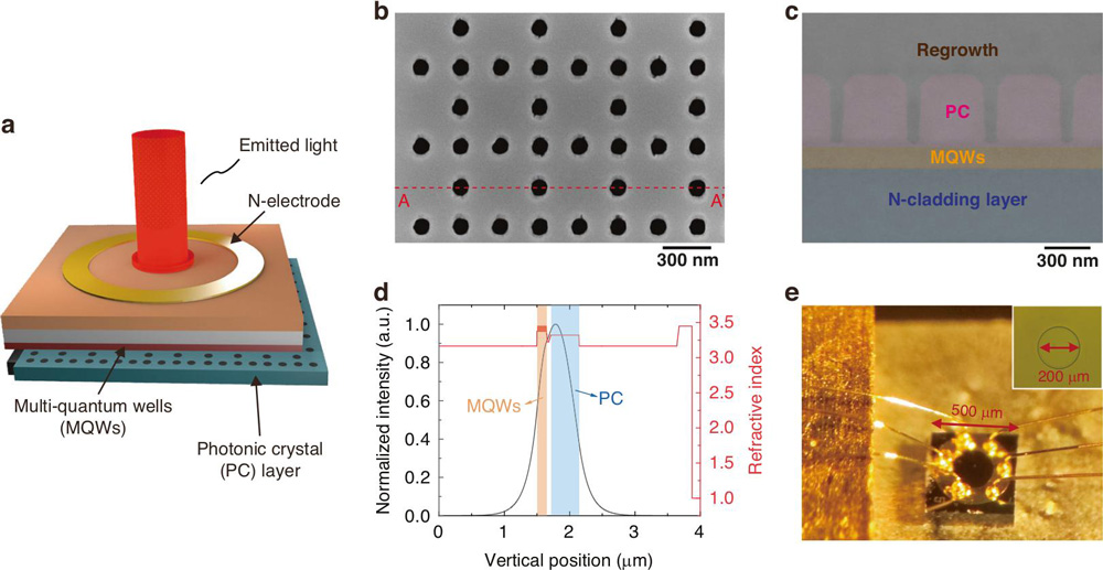
Figure 1: a PCSEL schematic. b Top-view scanning electron microscope image of triple-lattice photonic-crystal resonator. c Cross-sectional SEM image of resonator after epitaxial regrowth. d Refractive index profile and corresponding optical field distribution along crystal growth direction. e Images of laser chip bounded to thermally conductive submount with p-side down. Inset: p-side of chip.
The material for the device (Figure 1) was grown by metal-organic chemical vapor deposition (MOCVD) on n-InP substrate. The multiple quantum well (MQW) active region consisted of indium aluminium gallium arsenide (InAlGaAs) grown on an n-InP cladding layer. The first growth sequence was completed with a p-InAlAs electron-blocking layer and p-InAlGaAs.
The photonic crystal consisted of a square lattice of three offset holes, created by electron-beam lithography and inductively coupled plasma etch to a 375nm depth in a square 300μm region. The holes were filled by MOCVD regrowth of low-dielectric-constant InP.
This was followed by 50nm p-InAlGaAs and then 30nm grading to the p-InP cladding layer. The material structure was completed with p-InGaAs for the contact layer.
The photonic crystal holes were 90nm diameter. The photonic lattice constant was 474nm. The holes were arranged with a view to maximizing the 180° coupling to the optical field of the PCSEL. The mutual interaction of the nested lattices increased the 180° coupling threefold with respect to that of a single-lattice case, according to the team.
The researchers add: “The data show that the enhancement of the in-plane optical feedback significantly reduces the lasing threshold compared with the double-lattice PCSELs.”
The PCSELs were fabricated with substrate thinning to 180μm, circular mesa etching, 300nm silicon dioxide electrical insulation, and a 200μm-diameter reactive-ion etched circular contact window. The p- and n-electrode metals were, respectively, titanium-platinum-gold and nickel-gold/germanium-nickel-gold.
The device was mounted p-side down on copper.
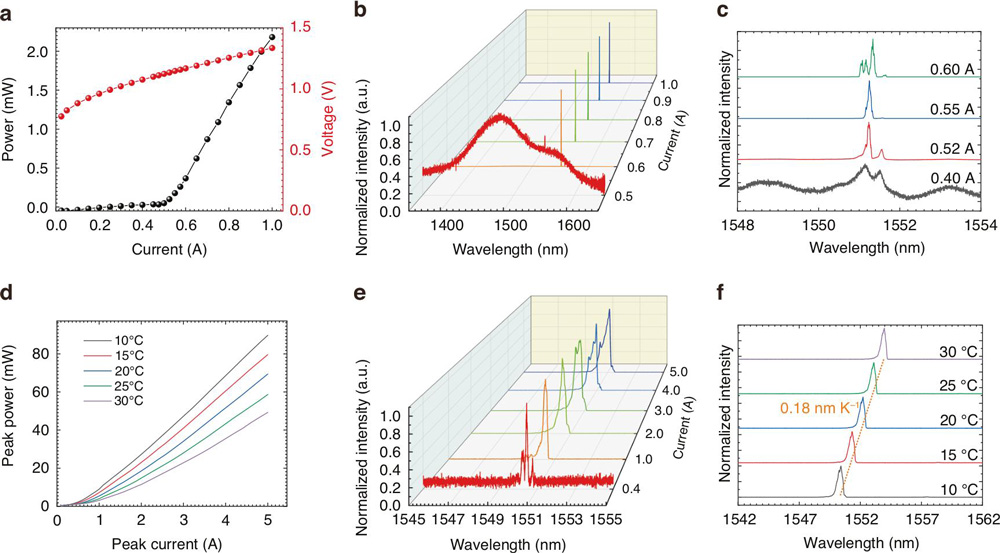
Figure 2: a Light–current–voltage characteristics under continuous-wave (CW) conditions at 10°C. b Emission spectra at various CW injection currents. c Magnified spectra near peak wavelength around threshold. d Light–current characteristics at various temperatures under pulsed conditions. e Emission spectra of pulsed lasers at various injection currents at 10°C. f Temperature dependence of emission spectra at 1A.
The output power of the device reached 2.1mW at 1A CW current injection (Figure 2). The threshold current was 0.52A (1.66kA/cm2 density). Spectra over the range 1350–1650nm showed emissions only around the 1551nm target wavelength. Above 0.6A injection the emissions were multi-mode. The maximum output power was 89mW with 5A pulsed current injection.
Table 1: Recent ~1.5μm PCSEL achievements. Top line is PCSEL in this report.
Year |
Wavelength (μm) |
Threshold |
Maximum output power (mW) |
Slope efficiency (W/A) |
Structure |
| 2023 | 1.55 | 1.66kA/cm2 | 89 | 0.02 | all-semiconductor |
| 2023 | 1.55 | 2.0kA/cm2 | 120 | 0.056 | void-containing |
| 2022 | 1.56 | 180 mA | 12.58 | 0.016 | Fabry–Pérot coupled |
| 2020 | 1.52 | 1.6kA/cm2 | 0.5 | 0.002 | void-containing |
The researchers also present a comparison with recent achievements in PCSEL research in this wavelength range (Table c).
PCSEL LiDAR InP p-InAlGaAs p-InGaAs MOCVD
https://doi.org/10.1038/s41377-024-01387-4
The author Mike Cooke is a freelance technology journalist who has worked in the semiconductor and advanced technology sectors since 1997.